Spi timing fpga module code speedgoat protocol diagram clock divider Spi timing Vhdl spi receiver
SPI Response Timing Diagram | Download Scientific Diagram
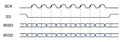
Schematic timing diagram of a serial peripheral interface (spi) data
Introduction to fpga configuration of adc through spi (2) -------- 4
Spi troubleshooting, teensy, arduino, and tri-stateSpi timing frame diagram speedgoat consists complete Spi modes mode notes readingSpi timing diagram arduino ece mode look.
Ccs/msp430fr2633: spi timing diagramSpi protocol Spi usage notes / spi / fpga code modules / fpga technology / speedgoatRace condition.

Spi timing diagram clock device pic
Introduction to spi interface and protocolSpi timing diagram Lmk04828: spi 3-wire read timingSpi timing greater cs intan blackfin.
Spi protocol timing diagram slave example master communicateSpi master and spi slave protocol communication support for simulink Spi protocolVerilog spi timing simultaneously happen decide events does when stack.

Spi timing nordicsemi infocenter
Timing spiReading list Spi timing diagram vhdl transmit only receiverAdvanced data acquisition techniques with ni r series.
Spi timingSpi protocol timing About spiSpi — serial peripheral interface master.

Spi command and response timing diagram
How to understand the spi clock modes?Spi (serial & peripher... Images of spiInterfacing with spi devices, part 1.
Spi timing álvarez danielSpi (serial peripheral interface) Spi mode 0 timing diagram....Spi timing configuration fpga adc introduction analysis line through write diagram figure.

Embedded system engineering: arm cortex-m3 (stm32f103) tutorial
Spi protocol clock read edge diagram timing data when pro communications introduction maker rising ising figureSpi serial timing diagram interface peripheral Spi timing diagram mode latch shift thenAn ece blog: bit banging data with the arduino.
Spi response timing diagramAn introduction to spi communications protocol Command spi timingTiming diagram of the spi signals for the two modules.

Spi timing diagram ni communication techniques acquisition advanced data series input figure
Fongeye: spi modes reading notes .
.